PUBLICATIONS

Graphene quality indicators obtained by Raman spectroscopy have been correlated to the structural changes of the graphene/germanium interface as a function of in-vacuum thermal annealing. Specifically, it was found that graphene becomes markedly defective at 650 °C. By combining scanning tunneling microscopy, X-ray photoelectron spectroscopy and near edge X-ray absorption fine structure spectroscopy, we concluded that these defects are due to the release of H2 gas trapped at the graphene/germanium interface. The H2 gas was produced following the transition from the as-grown hydrogen-termination of the Ge(1 1 0) surface to the emergence of surface reconstructions in the substrate. Interestingly, a complete self-healing process was observed in graphene upon annealing at 800 °C. The identified subtle interplay between the microscopic changes occurring at the graphene/germanium interface and graphene’s defect density is integral to advancing the understanding of graphene growth directly on semiconductor substrates, controlled 2D-3D heterogeneous materials interfacing and integrated fabrication technology.

We systematically investigate the chemical vapor deposition growth of graphene on Ge(110) as a function of the deposition temperature close to the Ge melting point. By merging spectroscopic and morphological information, we find that the quality of graphene films depends critically on the growth temperature improving significantly by increasing this temperature in the 910–930 °C range. We correlate the abrupt improvement of the graphene quality to the formation of a quasi-liquid Ge surface occurring in the same temperature range, which determines increased atom diffusivity and sublimation rate. Being observed for diverse Ge orientations, this process is of general relevance for graphene synthesis on Ge.
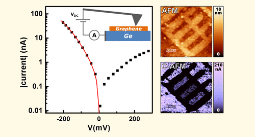
We report on the investigation of the Schottky barrier (SB) formed at the junction between a metal-free graphene monolayer and Ge semiconductor substrate in the as-grown epitaxial graphene/Ge(100) system. In order to preserve the heterojunction properties, we defined submicron size graphene/Ge junctions using the scanning probe microscopy lithography in the local oxidation configuration, a low-invasive processing approach capable of inducing spatially controlled electrical separations among tiny graphene regions. Characteristic junction parameters were estimated from I–V curves obtained using conductive-atomic force microscopy. The current–voltage characteristics showed a p-type Schottky contact behavior, ascribed to the n-type to p-type conversion of the entire Ge substrate due to the formation of a large density of acceptor defects during the graphene growth process. We estimated, for the first time, the energy barrier height in the as-grown graphene/Ge Schottky junction (φB ≈ 0.45 eV) indicating an n-type doping of the graphene layer with a Fermi level ≈ 0.15 eV above the Dirac point. The SB devices showed ideality factor values around 1.5 pointing to the high quality of the heterojunctions.
RELEVANT PUBLICATIONS PRIOR TO LIFEPLASTSENS
TUNING THE DOPING OF EPITAXIAL GRAPHENE ON A CONVENTIONAL SEMICONDUCTOR VIA SUBSTRATE SURFACE RECONSTRUCTION
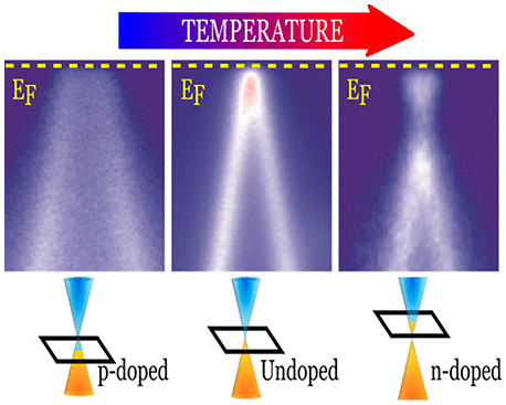
© 2021 American Chemical Society. Combining scanning tunneling microscopy and angle-resolved photoemission spectroscopy, we demonstrate how to tune the doping of epitaxial graphene from p to n by exploiting the structural changes that occur spontaneously on the Ge surface upon thermal annealing. Furthermore, using first-principle calculations, we build a model that successfully reproduces the experimental observations. Since the ability to modify graphene electronic properties is of fundamental importance when it comes to applications, our results provide an important contribution toward the integration of graphene with conventional semiconductors.
We systematically investigate the chemical vapor deposition growth of graphene on Ge(110) as a function of the deposition temperature close to the Ge melting point. By merging spectroscopic and morphological information, we find that the quality of graphene films depends critically on the growth temperature improving significantly by increasing this temperature in the 910–930 °C range. We correlate the abrupt improvement of the graphene quality to the formation of a quasi-liquid Ge surface occurring in the same temperature range, which determines increased atom diffusivity and sublimation rate. Being observed for diverse Ge orientations, this process is of general relevance for graphene synthesis on Ge.
We report on the investigation of the Schottky barrier (SB) formed at the junction between a metal-free graphene monolayer and Ge semiconductor substrate in the as-grown epitaxial graphene/Ge(100) system. In order to preserve the heterojunction properties, we defined submicron size graphene/Ge junctions using the scanning probe microscopy lithography in the local oxidation configuration, a low-invasive processing approach capable of inducing spatially controlled electrical separations among tiny graphene regions. Characteristic junction parameters were estimated from I–V curves obtained using conductive-atomic force microscopy. The current–voltage characteristics showed a p-type Schottky contact behavior, ascribed to the n-type to p-type conversion of the entire Ge substrate due to the formation of a large density of acceptor defects during the graphene growth process. We estimated, for the first time, the energy barrier height in the as-grown graphene/Ge Schottky junction (φB ≈ 0.45 eV) indicating an n-type doping of the graphene layer with a Fermi level ≈ 0.15 eV above the Dirac point. The SB devices showed ideality factor values around 1.5 pointing to the high quality of the heterojunctions.